Defining the Path to 400 Gbps‑per‑Lane Ethernet Signaling

Kent Lusted, Distinguished Architect, Synopsys
The Ethernet Alliance continues to serve as a vital forum for validating Ethernet technologies in real-world scenarios, as demonstrated during OFC 2026. In this guest blog, Kent Lusted, Distinguished Architect at Synopsys, discusses the path to 400Gbps-per-lane signaling.
Over the past year, the Ethernet community has examined 400Gbps‑per‑lane signaling from many angles: AI network use cases, modulation options, channel limitations, and technology feasibility. Those discussions have been necessary, but they now need to converge into decisions that allow the industry to move forward.
This article focuses on the next steps required to advance a 400Gbps‑per‑lane Ethernet project, and the recent study group announcement at OFC 2026.
Scoping the Work: Why “Effort #1” Matters
Multiple Ethernet standard development efforts are forming in parallel, each addressing different reaches, applications, or architectural assumptions. To make fast progress and address the time-to-market of end users, it is necessary to constrain scope.
The focus here is on Effort #1:
The set of applications where higher signaling rates are required first, and where industry alignment can be achieved most rapidly.
Other efforts, longer reach, alternative architectures, or different PHY optimizations, remain important. However, attempting to solve everything simultaneously would significantly delay progress. The intent of a multi-effort strategy is to start where the technical and market pressure is highest, then build outward.
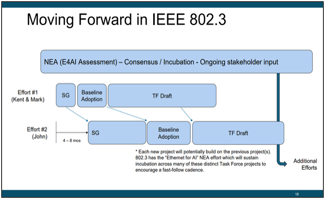
Figure 1. Two efforts forming in the pipeline Taken from: https://www.ieee802.org/3/ad_hoc/E4AI/public/25_0819/dambrosia_e4ai_01_250819.pdf
Market Driver: Scale‑Up AI Networks Lead the Need
The primary driver for 400Gbps‑per‑lane signaling is the rapid growth of AI back‑end, scale‑up networks for GPU to GPU communication.
These networks are characterized by:
- High‑radix switching
- Flat or minimally tiered topologies
- Large numbers of one-lane and two-lane links
- Strong sensitivity to latency, power, and port density
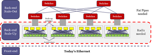
Figure 2. AI Data Center Network Hierarchy based on “AI Datacenters and their Diverse Network Requirements”, Ram Huggahalli (Microsoft), Ethernet Alliance TEF 2024, Oct 2024.
While scale‑out and front‑end networks will eventually benefit from higher lane rates, scale‑up networks experience the pressure first. They require higher bandwidth per lane to enable radix‑optimized designs without excessive port counts, cabling complexity, or power consumption.
This observation drives the central premise of Effort #1:
Start with scale‑up, short‑reach applications, and expand later.
Interconnect Reality: Copper Is Constrained, Not Obsolete
Copper interconnect remains attractive due to its:
- Lower cost
- Lower power consumption
- High reliability
- Mature manufacturing ecosystem
However, at 400Gbps per lane, reach is shrinking. Physics increasingly limits what passive copper can deliver, particularly as channel loss budgets tighten and margin disappears.
This naturally shifts attention toward active copper solutions, which introduce new considerations:
- Passive cables remain well understood and standardized but are limited to very short reaches.
- Active Electrical Cables (AECs), incorporating retimers, resemble pluggable optical modules from an Ethernet perspective and benefit from validation concepts.
- Active Copper Cables (ACCs), incorporating redrivers, occupy a less well‑defined space. Their behavior, performance expectations, and validation methodologies are not yet consistently specified across the industry.
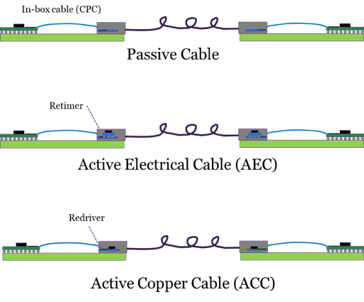
Figure 3. Reach limitations of passive copper emphasizes the need for active solutions
If ACCs are to play a role at 400Gbps per lane, the community must align on definitions, assumptions, and measurement approaches. Without that alignment, interoperability and scalability will be at risk.
At the 400Gbps per lane data rate, it is no longer sufficient to specify components in isolation—the entire electrical channel must be considered as a system.
Host Evolution: Electrical and Optical Are No Longer Separate Problems
In parallel with cable evolution, host system implementations are diversifying.
Where earlier Ethernet generations were dominated by PCB traces to front‑panel pluggable connectors, 400Gbps‑per‑lane systems are expected to include a mix of:
- Traditional PCB trace‑based designs
- Co‑packaged copper (CPC)
- Near-packaged copper (NPC)
- Near‑package optics (NPO)
- Co‑packaged optics (CPO)
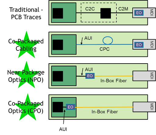
Figure 4. C2M Hosts for 400 G/lane
This diversity fundamentally changes the problem space. Electrical and optical interfaces can no longer be designed independently; their interaction determines system performance and reach.
At 400Gbps per lane, every element in the channel—package, host routing, connectors, cable assemblies, and optical interfaces—has a measurable impact on end‑to‑end performance. There is effectively no excess margin.
Electrical Interfaces: Modulation Depends on the Channel
A recurring question is whether the electrical interface should remain PAM4 or evolve to higher‑order modulation, such as PAM6 or PAM8.
The key point is that modulation choice is inseparable from channel assumptions.
The channel includes:
- Package and die‑to‑substrate transitions
- Host traces or co‑packaged cabling
- Front‑panel or near‑package connectors
- Cable or backplane assemblies
Experience from 112 G → 224 G signaling transitions has shown that as rates increase, small degradations anywhere in the channel have outsized effects. At 400 Gbps per lane, system optimization becomes an exercise in carefully trading margin between elements rather than allocating it independently.
You can learn more about 448G system optimization in this white paper: Improving COM Accuracy for 400G Ethernet.
This leads to a broader mindset shift, from “I need margin here” to “I can trade margin here to recover it elsewhere.”
Four Core Electrical Questions
The electrical work centers on four recurring themes:
- System Design
How many 400 Gbps‑per‑lane ports are assumed in switches, NICs, and accelerators? What is the expected mix of copper and optical connections? Are long‑standing assumptions about system architecture still valid? - Industry Readiness
Can new connectors, cables, and interconnect technologies meet performance targets at hyperscale volumes, not just in prototypes? - Modulation Alignment
How important is common coding between electrical and optical interfaces?
Are linear optical solutions—pluggable or co‑packaged—viable at 400 Gbps per lane, and on what timeline? - Validation Tools
Are test and measurement solutions ready to validate PAM4/6/8 signaling at scale, with repeatability and confidence?
Optical Interfaces: Fast Progress, Conditional Assumptions
Historically, optical Ethernet interfaces have progressed more quickly than their electrical counterparts, with electrical specifications following shortly thereafter. That pattern may hold again—but only if assumptions are examined early.
There is emerging alignment around PAM4 optical modulation as the leading candidate for the targeted reaches in Effort #1. However, optical performance depends heavily on:
- Host electrical assumptions
- Connector quality
- FEC architecture
- Power and thermal constraints
Effort #1 assumes that both pluggable optics and CPO will coexist, rather than selecting one exclusively. This places additional emphasis on interoperability and on choosing starting points that do not preclude future implementations.
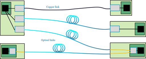
Figure 5. Seamless Interoperability: An Ethernet Expectation
For single‑lane optics, single‑mode fiber appears to be a relatively benign channel, with a reach on the order of ~500 m serving as a useful reference point. Whether that number should be shorter or longer depends on detailed power, cost, and yield trade‑offs that must be evaluated.
As with electrical interfaces, test methodologies for optics must be addressed early to avoid downstream delays.
FEC and PCS: The Electrical–Optical Boundary
FEC and PCS sit at the intersection of electrical and optical signaling.
Historically:
- Modulation commonality (NRZ→NRZ, PAM4→PAM4) enabled linear optical solutions.
- Copper channel behavior drove the selection of burst‑tolerant FEC schemes such as RS(544).
- Optical implementations often reused those codes or added inner FEC layers.
At 400Gbps per lane, these assumptions deserve re‑examination.
Key questions include:
- Does RS(544) scale appropriately for high‑radix, single‑lane use cases?
- Should a new FEC be considered that better balances error correction, latency, and implementation complexity?
- How do interleaving choices affect latency in radix‑optimized AI networks?
FEC is no longer just a reliability tool, it is a system‑level performance lever.
Project Focus: What Effort #1 Intends to Deliver
The initial 400Gbps‑per‑lane effort is expected to focus on:
- Existing Ethernet MAC rates:
- 400GbE (x1)
- 800GbE (x2)
- 1.6TbE (x4)
- New 400Gbps‑per‑lane PHYs and interfaces:
- Copper cable and backplane (passive and active), reach TBD
- Optical single‑lane SMF (parallel SMF), reach ≈ 500 m
- Electrical chip‑to‑module (C2M) and chip‑to‑chip (C2C) interfaces
Constraining the scope in this way is essential to manage complexity and timeline.
Summary
400 Gbps‑per‑lane signaling represents a step change in Ethernet design, driven primarily by AI scale‑up networks and their unique architectural demands. The work is now underway in the newly formed IEEE 802.3 400 Gbps per lane signaling Study Group.
Success will require:
- Early, disciplined scoping
- Tight integration of electrical, optical, and FEC/PCS considerations
- A willingness to make initial decisions and refine them as data emerges
- Focus on interoperability across copper, pluggable optics, and CPO
Effort #1 is not about solving every future problem—it is about starting in the right place, with the right assumptions, and moving forward together.
The views and opinions expressed are those of the authors and do not necessarily reflect the official policy or position of the Ethernet Alliance.