A Deep Dive into the 802.3bs 200GBASE-R and 400GBASE-R PCS/PMA

The Physical Coding Sublayer (PCS) is responsible for the encoding of data bits into code groups for transmission via the Physical Medium Attachment (PMA) and the subsequent decoding of these code groups from the PMA. For the 802.3bs architecture, it was decided to reuse the low‐overhead multilane distribution scheme from 802.3ba and the transcoding and RSFEC from 802.3bj for the PCS for 200 Gigabit Ethernet (200GbE) and 400 Gigabit Ethernet (400GbE).
The PCS has been designed to support all PHY types for both 200GbE and 400GbE. It is flexible and scalable, and can possibly support future PHY types that may be developed, depending on FEC gain needs of the new interfaces. The PCS layer performs the following functions:
- Delineation of frames
- Transport of control signals
- Ensures necessary clock transition density needed by the physical optical and electrical technology
- Strong Forward Error Correction (FEC) to control errors in a high BER environment
- Stripes and re‐assembles the information across multiple lanes
The transmit PCS performs the following major functions in order:
- Performs the initial 64B/66B encoding
- Transcodes 4×66-bit blocks to a single 256B/257B block
- Scrambles the stream with X^58 scrambler
- Alignment markers are periodically added
- Distributes the data to two FEC engines (10-bit round robin)
- Two parallel FEC codewords are formed by performing Reed-Solomon Encoding on the data
- The two codewords are then played out in a 10-bit round robin distribution to the 8 (200GbE) or 16 (400GbE) PCS lanes
- The PMA can bit multiplex down to less lanes for a given AUI or PMD interface
This PCS leverages the 64B/66B coding scheme that was originally used in 10 Gigabit Ethernet, but also transcodes a group of four 66-bit codewords down to 256B/257B codewords to further reduce the coding overhead and to create extra room for FEC. The transcoding is similar to that first supported in 100GbE with the 802.3bj standard, with the exception that transcoding is performed before scrambling for 200/400GbE (to simplify the transcoding).
The PCS then scrambles the data after transcoding to ensure sufficient transitions and to control baseline wander. The scrambling includes the 257th bit of each transcoded blocks since it would otherwise lead to a decrease in randomness. After the data stream is scrambled, alignment markers are then added into the stream so they will appear periodically on each PCS lane. This allows the receive PCS to deskew and reorder the lanes. Note that the alignment markers are processed pre FEC correction since deskew and reordering must occur before FEC correction can occur.
The single datastream is then split into two streams, with a 10-bit round robin distribution, which feeds two FEC instances. Each FEC instance will perform Reed-Solomon encoding on its data into a (544,514,T=15,M=10) codeword. Each codeword can correct up to 15×10-bit symbols when processed in the receive PCS. After two codewords are created, the data is distributed to the PCS lanes by doing a 10-bit distribution from the two FEC codewords, it creates a checkboard pattern as shown in Figure 1.
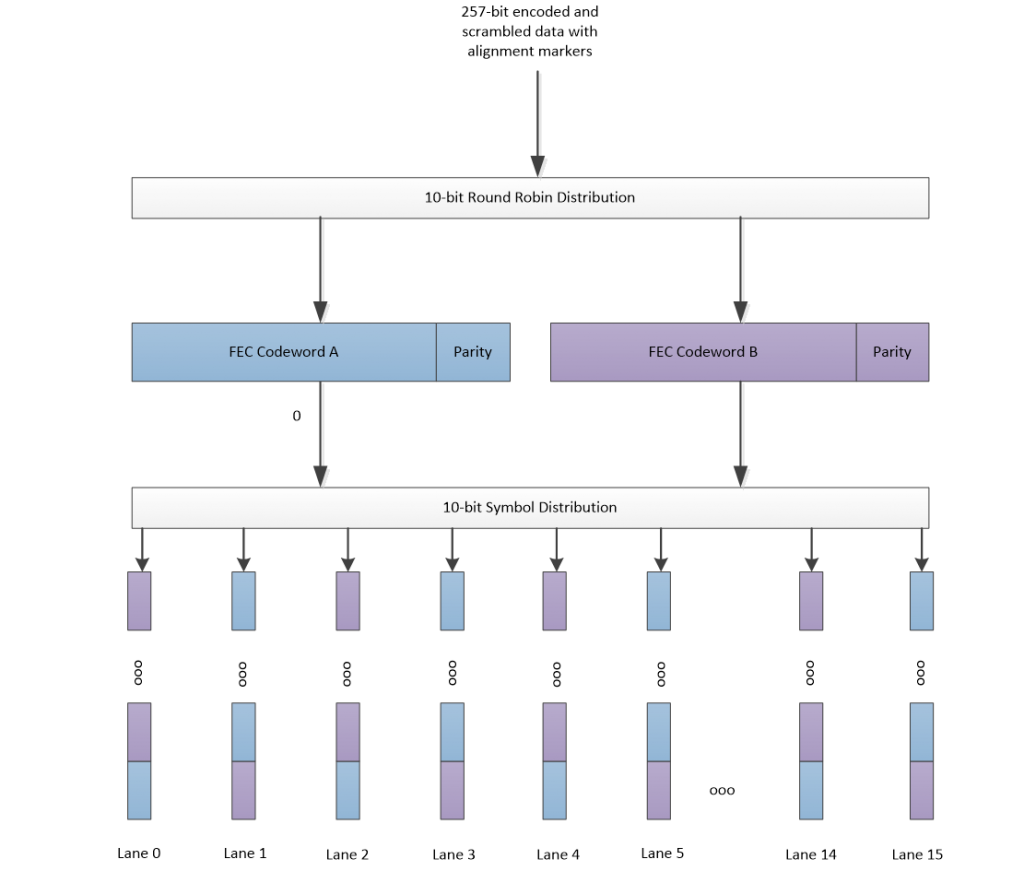
Figure 1 TX Data Distribution
The above functions provide the following properties: very low overhead and sufficient code space to support necessary code words, many clock transitions and controlled baseline wander, an alignment mechanism for the multilane interface, and a strong FEC to control errors.
The number of PCS lanes needed is the least common multiple of the expected widths of optical and electrical interfaces. For 200GbE, 8 PCS lanes have been chosen. Therefore, 8 PCS lanes support interface widths of 1, 2, 4, and 8 lanes or wavelengths. For 400GbE 16 PCS lanes support interface widths of 1, 2, 4, 8 and 16 lanes or wavelengths.
Once the PCS lanes are created they can be multiplexed into any of the supportable interface widths. Each PCS lane has a unique alignment marker, which is inserted once every 81,920 257-bit blocks for 200GbE, and 163,840 257-bit blocks for 400GbE. Room for alignment marker insertion is created by deleting idle characters (or not inserting them in the first place). All multiplexing is done at the bit‐level. The round‐robin bit‐level multiplexing can result in multiple PCS lanes being multiplexed into the same physical channel. The unique property of the PCS lanes is that no matter how they are multiplexed together, all bits from the same PCS lane follow the same physical path, regardless of the width of the physical interface. This enables the receiver to correctly re‐assemble the aggregate channel by first de‐multiplexing the bits to re‐assemble the PCS lane and then re‐align the PCS lanes to compensate for any skew.
The alignment markers are shown in Figure 2. The format is partially compatible with that of the 100GbE 802.3bj markers, in that the first two groups of common bytes are identical between the standards (CM0-CM5). The common markers are also identical on each lane, this allows the logic to lock to the markers without worrying about the lane number, and after the markers are located then each individual lane is identified by the unique marker portion (UM0-UM5) which are unique across the lanes. The padding is unique per lane but ignored on receive.
![]()
Figure 2 Alignment Marker Format
The receiver PCS realigns multiple PCS lanes using the embedded alignment markers and then re‐orders the lanes into their original order to reconstruct the aggregate signal. The alignment markers are processed before FEC correction, and so are processed in a manner that allows mismatches in some bits of the alignment markers.
Two key advantages of the PCS multilane distribution methodology include the encoding, scrambling, and de‐skew functions can all be implemented in a CMOS device (which is expected to reside on the host device), and minimal processing of the data bits (other than bit muxing) happens in the high speed electronics embedded with an optical module. This simplifies the functionality and ultimately lower the costs of these high‐speed optical interfaces.
The PMA sublayer enables the interconnection between the PCS and any type of PMD sublayer. A PMA sublayer will also reside on either side of a retimed interface, referred to as “200GAUI” (200 gigabit per second attachment unit interface) for 200GbE or “400GAUI” (400 gigabit per second attachment unit interface) for 400GbE. The transmitter PMA provides signal drivers, bit multiplexing, PAM4 encoding when appropriate (8 or fewer lanes), Gray coding and precoding when desired. The receiver PMA provides clock and data recovery, bit demultiplexing, and PAM4. The receiver PMA provides clock and data recovery, bit demultiplexing, and PAM4 decoding.
As described in the previous section, 16 PCS lanes are used for 400GbE. In the example implementation shown in Figure 3, the two PMA sublayers are interconnected by the 400GAUI electrical interface, which is based on an 8 lane wide interface at 50 gigabit per second per lane. In this implementation the PMA sublayer at the top of the 400GAUI multiplexes the 16 PCS lanes into 8 physical lanes. The PMA sublayer at the bottom of the 400GAUI performs multiple functions. First, it retimes the incoming electrical PAM4 signals, then the electrical lanes are converted back to 16 PCS lanes, which are then multiplexed into the 4 lanes needed for the 400GBASE‐DR4 PMD.
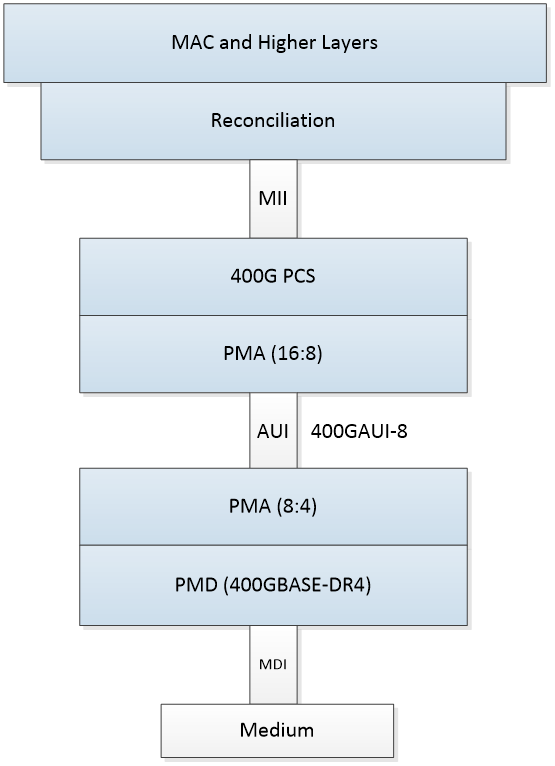
Figure 3 400GbE Example Protocol Stack
One new PCS feature for these interfaces is the ability to support a FEC degraded signal. This allows the user to set a threshold of corrected FEC symbols within a specified period, and if a threshold is passed the PCS can declare a degraded condition. This FEC degraded signal can be used by higher protocol layers to take proactive actions such as cause a route switchover.
The PCS in combination with the PMA has been created to support all PHY types for both 200 Gigabit Ethernet and 400 Gigabit Ethernet. It is flexible and scalable, and can support future PHY types that may be developed in the near future.