Technical Feasibility: Next Generation Optical Interfaces – TEF21 Panel Q&A – Part 1

Mark Nowell, Ethernet Alliance advisory board chair and Cisco![]()
Scott Schube, Intel
Matt Traverso, Cisco Systems
David Lewis, Lumentum
Xinyuan Wang, Huawei
The optical technology industry is heading into a time of transition. As 100G per lambda technology matures and is established as a key building block for networks and the question becomes, what are the next steps for the industry to consider? Day four of TEF21: The Road Ahead conference focused on new directions for next-gen optical interfaces in the session Technical Feasibility: Next-Generation Optical Interfaces. Moderator and Ethernet Alliance Board Advisory Chair Mark Nowell, Cisco, and panelists David Lewis of Lumentum (Performance Photonics Enabling Next Generation Interfaces); Scott Schube of Intel (Scaling Bandwidth with Optical Integration); Matt Traverso, Cisco (Scaling Architecture for Next Gen Optical Links); and Huawei’s Xinyuan Wang (Observations on the Rate of Beyond 400GbE, 800GbE and/or 1.6TbE) shared their views on those transitional next steps including speeding up the building blocks to support the next rates, understanding how to re-package technologies to enable co-packaged optics and understanding the trade-offs between direct detect and coherent technologies.
Afterwards the audience asked panelists numerous questions about the future of optical interfaces. Their insightful responses are captured below in part one of a two-part series.
 Cost per bit advantages – lasers or photonics?
Mark Nowell: It has been suggested that with the integrated laser as you scale to wider and wider lanes, the costs (per bit) become less and less. But is the full integration a much higher cost? Can you talk about that and discuss whether there’s an optimum in terms of this lane width?
Scott Schube: I think it does depend on implementation and the key caveat here is for sufficiently high yield process technology. This is based on our projections. Obviously, the sweet spot depends on a yield per lane and concatenated yield per lane so your ‘mileage may vary’. The point of your question is whether there is a point where even for the fully integrated approach the cost per bit starts to creep up and for sure there is. You can’t extend this out to 1,000 lanes of optics, for instance, without it becoming infeasible. Based on our analysis even at high lane counts, there are cost per bit benefits to be achieved.
Mark Nowell: Discrete and silicon photonics are equally effective when only a single lane is required. Does silicon photonics have any advantage for machines that only need a single lane, such as servers?
Scott Schube: The advantage is smaller for sure at single lane versus multiple lanes and there are some other advantages depending on implementation. Not necessarily integration as a general rule but there may be quality advantages. There may be manufacturing scale advantages or other things that come into play that give an advantage of a silicon photonics-based approach with single lane. But in terms of generally looking at integrated optics, at single lane the differences shown is much less.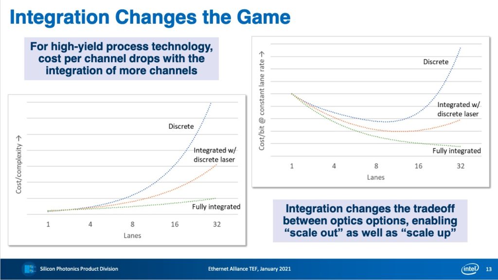
Mark Nowell: It has been suggested that integrating the lasers provides a much more scalable platform from a width perspective, but also that it really isn’t a free lunch because of noise and cross talk issues. Do you think there’s a limit in terms of width or an optimum in terms of width?
Matt Traverso: That’s a good question and I don’t know. I think it depends a little bit on the technology choice and implementation. There are implementations where the electrical die is flip chipped on to the optical die and the corresponding electrical interconnect are copper pillars which are at 80 micron pitch. So it comes down to what is my driver implementation, what is my TIA implementation and how can I get those close together. And for flip chip technology, it’s just important to be at a realm that’s consistent with the rest of the OSAT (assembly and test) capability. We have found that 80 microns is a reasonable place to be. Tighter than that gets tough.
Matching lane rates to optical lanes
Mark Nowell: The options of 800GbE and 1.6Tb Ethernet from a system perspective, when you look that and look at what the IEEE is about to try and do, when you look from an optical perspective, what do you think the priority should be for that group? Is it focusing on 100G lanes or 200G lanes?
Xinyuan Wang: I think for the 10km, it should be based on the coherent 800G per lane solution. Either optical solution should be work together based with logic layer solution. The logic layer solution should be friendly to support all of the different optical solutions. And if we talk about the 2026 that the standard would be published, 200G solution should be good for the 2km application.
Mark Nowell: We’ve talked about scaling in terms of wider lanes and going faster and had a lot of discussions around what that network or the user needs are around radix lanes, which are getting wider. In terms of the width of the lanes or the amount of integration, does that affect our need to go to 200G? What are your thoughts about when 200G lanes are going to be needed optically?
Scott Schube: I think in general – although obviously optics feasibility and preferences and technology influence decisions – we try to have optics ready to be there when the next switch generation is available. So a simple answer might be to go to 200G per lane when there’s switches that come out with 200G per lane out of the switch. I don’t think a reverse gearbox approach or anything like that to stay at 100G on the optics while the switch is at 200G per lane makes sense. But until then, I think 100G per lane should meet the needs.
Matt Traverso: we should line up to the capabilities of the analog electronics. I think that’s really going to be key for our next generation, even more than the optical devices themselves. And it’s that co-packaging and that integration that becomes key for how we put the whole thing together.
Dave Lewis: Yeah. I would say whether it’s co-packaged or any other type of packaging, the important thing is to match the lane rates to the optical lanes. Gearboxes and muxes are useful in intermediate solutions, but they’re never really the lowest cost. So, if you’ve got a 100G per lane optical device but the switches were 50G per electrical lane, then you’ve got to match everything up and it’s extra components, extra power consumption. It’s not really solving the problem. I think once we have the switch chips that have 200G lanes then we’ll see 200G per lane optics. On the other hand, there are other applications and switches but they may not be Ethernet. 200G could be used in other machine learning, AI applications where there is no Ethernet switch necessarily. So we’ll see what comes down the pipe. But for now, I think with IEEE hats on it’s really all the pieces need to be there. What we typically end up with is a MAC that puts the signal on to a certain number of lanes and as long as those lanes are the right subdivision of the optical lane, everything works quite well. I’d suggest, you know, 50 or 100G is the sort of base unit of an interface.
Mark Nowell: We’ve often seen in the industry that the optical lanes are actually ahead of the electrical lanes. With 400G we’re still at an 8 X 50 but we’re at 4 X 100 optically. Am I then to interpret from the discussion so far that you think that the shift to 200G optical lanes is really going to be tightly coupled with the shift to 200G electrical lanes? Or are we going to wait for the electrical lanes?
Dave Lewis: My answer was that if you look at today’s 8 X 50 electrical with a 4 X 100 optical interface on it, that’s an intermediate step towards 4 X 100 electrical, 4 X 100 optical which we don’t quite have yet, right.
Xinyuan Wang: I think in the previous discussion, we talk about what’s evolution for the Ethernet standard. And someone talked about follow the SerDes. I agree most of this discussion. The same rate from electrical and optical may be the best solution for the long-term. Or maybe we got the 200G SerDes electrical in the switch ASIC, then 200G optical lane maybe work together and it is best. And also, we should consider supporting earlier availability. Maybe someone is interest in the 2X100G electrical to multiplex to 200G Lane. I think this is also discussed in the last year, 2020, when we prepared the CFI. It is also discussed as one of possible early solution.
Mark Nowell: One last question on lane rates, looking at high speed electrical technology, there’s a lot of discussion around the different paths to 200Gs or 224G looking at the different modulations, PAM4, PAM6, PAM8. Do you think there needs to be a similar study within the optical interfaces around the modulation rate? Or is there less latitude there with the optical technology?
Matt Traverso: I think it really comes down to what is the output of that serializer and what is that clock and data recovery. I think we have a lot of flexibility as far as, like, coding scheme and what modulation we go do. But really, it’ll come down to that clock recovery to get a good decision at the digital interface. We of course have additional noise that comes in because of the optical environment, but some things are easier. We can use multiple wavelengths and achieve pretty easily and do things like bidirectional much more easily in the optical domain than you can in the electrical domain. But fundamentally, it’ll come down to that decision in circuitry in my opinion.
Scott Schube: There definitely are different tradeoffs. In general, the optical devices although for sure bandwidth is always a challenge, it seems to be less of a challenge than these long electrical channels that folks were talking about. But the SNR is a tougher challenge. I think in general it kind of nudges towards less levels. That doesn’t necessarily mean that it’s impossible to do something with more levels, but that’s definitely harder for optics and the tradeoff is probably more towards less levels than it would be on the electrical side, so we have to see.